


 tel:+86-18825224069
 email:
 address:201, Factory 6, Longhui Industrial Park, Fuqiao 3rd District, Xinhe Community, Fuhai Street, Baoan District, Shenzhen china
What are the most commonly used PCB equipment for beginners?
Release date:2022-06-24 17:34:34 Number of views:0

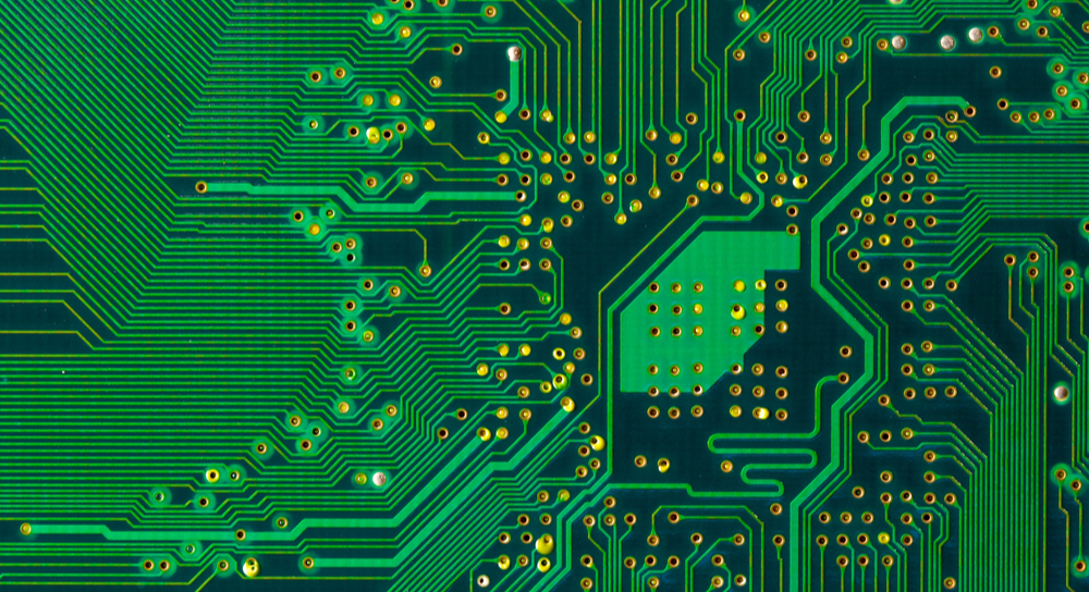
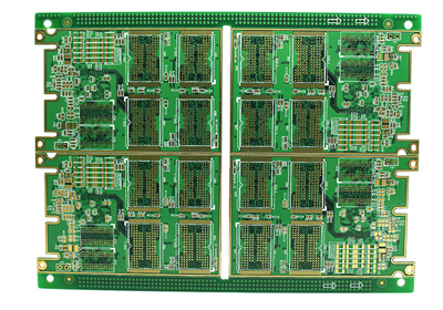
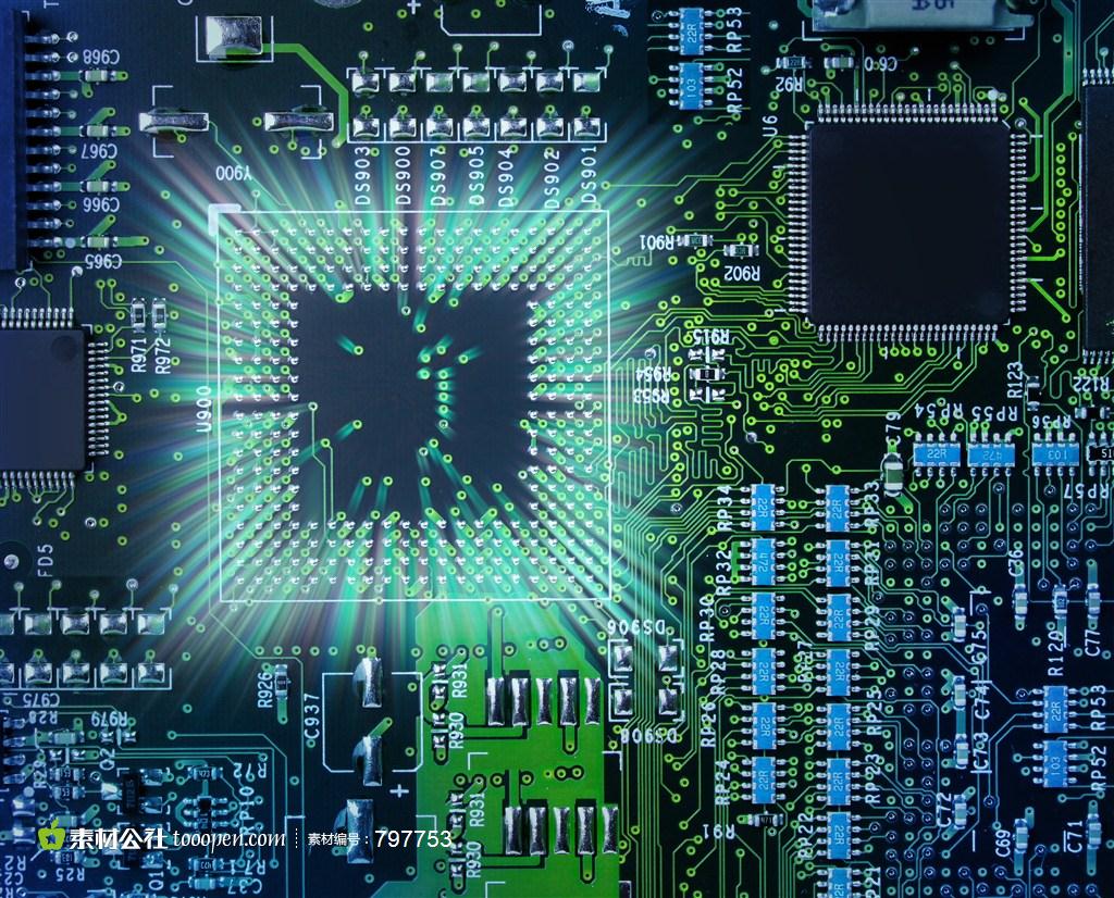
PCB equipment is a device for producing circuit boards, which belongs to the equipment producing circuit boards, including vacuum packaging machines, gluing machines, and developing machines. The PCB equipment includes deburring machine, a double-sided alkaline etching machine, a metal chemical cleaning machine, etching production line.
Today, when society is approaching the age of electronics and automation, as well as the wave of investment in electronic manufacturing from abroad, the demand for electronic boards and components is increasing day by day growing rapidly. At this time, owning a factory manufacturing circuit boards, PCBs, boards, and electronic circuits is almost like owning a "money printing machine". However, how to have a standard and quality PCB factory, not all investors know!
What includes in PCB equipment?
The PCB equipment includes deburring machine, double-sided alkaline etching machine, metal chemical cleaning machine, etching production line...
The deburring machine is mainly used for special equipment for removing drilling burrs, surface oxide layers, and purifying the surface of printed circuit boards. The 30Kg/cm2 high-pressure cleaning pump can completely remove drilling burrs and surface dirt,
Classification
1. PCB pre-fabrication equipment
-PCB electronic film developer, fixer-automatic film processing machine
- Machine nozzles for developing, electroplating, etching, film removal, etc.
2. PCB machining equipment
-Vacuum laminator, vacuum lamination machine -PCB substrate grinding machine-PCB forming machine-PCB inner layer fusion machine-automatic alignment fusion machine-PCB lamination machine
3. Electroplating/Wet Process Equipment
-Development of etching stripping-chemical nickel gold production line-PCB assembly line
4. Screen printing/drying process equipment
-Provide a variety of UV curing machines -Precision hot air oven, oven-Human machine interface UV curing machine-
Involves more than a dozen processes, and each process involves an average of about 5 devices. Electroplating line, immersion copper wire, DES wire, SES wire, cleaning machine, OSP wire, immersion nickel gold wire, press, exposure machine, oven, AOI, plate warping leveling machine, edge grinding machine, cutting machine, vacuum packaging machine, gong machine, drilling rig, air compressor, tin spraying machine, CMI series, photoplotter.

pcb equipment column
Introduce several important types of equipment, others are not listed one by one
Fully automatic placement machine: It is fully automated online placement equipment. It is a device that accurately places surface mount components in a fixed position through an automatically moving placement head. The positioning has a mechanical alignment, and visual.
There are several ways of alignment and laser alignment. This equipment is indispensable key equipment in SMT production.
Manual placement machine: It is completely manual, using vacuum nozzles and guide rails to achieve component placement. The advantage is that the price is economical and easy to use. The disadvantage is that the positioning accuracy is poor, the speed is slow, and it cannot adapt to the PCB assembly with high assembly density.
This equipment is more suitable for the research and development and production of small batches and varieties of scientific research institutions, research institutes, various electronic laboratories, etc.
Fully automatic screen printing machine
It is fully automated online screen printing equipment, which realizes the missing printing of solder paste or patch glue through automatic machinery. The positioning is basically through the way of optical alignment; the operator can control the movement of the scraper through the electronic control switch or control the equipment through programming.
This equipment is characterized by high speed, high positioning accuracy, and ease to use. The disadvantage is that it is expensive and relatively difficult to maintain. It can adapt to PCB assembly with high assembly precision and large-scale mass production.
Semi-automatic screen printing machine
It is a kind of equipment between a manual screen printing machine and an automatic screen printing machine, which realizes the missing printing of solder paste or patch glue through machinery. There are two ways of positioning: complete manual positioning and optical alignment.
The operator can control the movement of the scraper through an electric control switch. The features of this device are affordable and easy to use. The disadvantage is that the speed is slow, the positioning accuracy is not high, and it cannot adapt to the PCB assembly with high assembly accuracy and large-scale mass.
Manual screen printing machine: simply called "manual screen printing table", it is completely manual to realize the missing printing of solder paste or patch glue. The advantage is that the price is economical and easy to use. The disadvantage is that the positioning accuracy is poor, and it cannot adapt to some PCB assemblies with high assembly density.
Design in PCB
There is no such thing as a standard PCB. Each board has a unique function for a specific product and must be designed to perform that function in an allocated space. Board designers use computer-aided design systems with special software to lay out the schematic on the board.
The spaces between conductive conductors are typically 1.0 mm or less. Holes for component wires or contact points are also placed, and this information is translated into instructions for a computer numerically controlled drilling machine or an automatic soldering iron used in the manufacturing process.
Once the circuit diagram is laid out, a negative image or mask is printed on a transparent plastic sheet. When negative, areas that are not part of the circuit are shown in black, and the circuit is shown as transparent.
Raw material
The substrate most commonly used in PCBs is glass fiber reinforced epoxy (fiberglass) with a copper foil bonded to one or both sides. Substrates made from paper-reinforced phenolic resin with bonded copper are less expensive and are often used in household electrical applications.
Printed circuits are made of copper, which is either plated or etched onto the surface of the substrate to leave the desired pattern. Copper chains are coated with tin-lead to prevent oxidation. The contact fingers are plated with tin-lead, then nickel, and finally gold for excellent conductivity.
Purchased components include resistors, capacitors, transistors, diodes, integrated circuits, and others.
Production process
PCB processing and assembly are carried out in an extremely clean environment where air and components can be free from contamination. Most electronic manufacturers have their processes, but in general, the following steps can be used to make a double-sided PCB.
Woven fiberglass is unwound from a roll and fed through a processing station. The illustrations above show an enlarged section of the PCB. The illustrations above show an enlarged section of the PCB. where it is impregnated with epoxy either by dipping or spraying. The impregnated fiberglass is then passed through rollers which roll the material to the desired thickness of the finished substrate and also remove any excess resin.
Drilling and covering holes
Several substrate panels, each large enough to make several circuit boards, are stacked on top of each other and secured together so that they do not move. The folded panels are placed in a CNC machine and holes are drilled according to the pattern determined when laying out the boards. The holes are separated to remove excess material adhering to the edges of the holes.
The inner surfaces of the holes, designed to provide a conductive loop from one side of the board to the other, are copper-plated. Non-conductive holes are connected so that they are not covered. PCB or drilled after the individual boards are cut from the larger panel.
Create a printed circuit pattern on a substrate
A printed circuit design may be created through an "additive" process or a "subtractive" process. In the doping process, copper is plated or added to the surface of the substrate in the desired pattern, leaving the rest of the surface untreated. The subtraction process first covers the entire surface of the substrate, and then areas that are not part of the desired pattern are etched or subtracted. Let us describe an additive process.
The surface of the backing foil is degreased
The panels pass through a vacuum chamber where a layer of positive photoresist material is pressed tightly against the entire surface of the foil. A positive photoresist material is a polymer that can become more soluble when exposed to ultraviolet light.
The vacuum ensures that there are no air bubbles between the foil and the photoresist. The printed circuit template mask is laid over the photoresist and the panels are exposed to intense UV light. Since the mask is transparent in areas of the printed circuit pattern, the photoresist in these areas is irradiated and becomes very soluble.
The panels are then galvanized with copper
The foil on the surface of the substrate acts as a cathode in this process and the copper is plated in the exposed areas of the foil with a thickness of about 0.025-0.050 mm. Areas still coated with photoresist cannot act as a cathode and are not coated. Tin-lead or other protective coating is applied on top of the copper plating to prevent oxidation of the copper and as a resist for the next step in production.
The photoresist is removed from the boards with a solvent to expose the copper foil of the substrate between the coated printed circuit patterns. The boards are sprayed with an acidic solution that eats away the copper foil. The copper plating on the printed circuit is protected by a tin-lead plating and is not attacked by acid.
Comment on this article here
-
No comment

Ripple
Hi everyone, I'm Ripple, Sales Director of KFPCBA Tech Ltd. If you are looking for a one-stop PCB and PCB assembly manufacturer in China, KFPCBA is your best choice! Please feel free to contact our team! Thanks!
Contact me now


