



 tel:+86-18825224069
 email:
 address:201, Factory 6, Longhui Industrial Park, Fuqiao 3rd District, Xinhe Community, Fuhai Street, Baoan District, Shenzhen china
SMT Assembly Process Explained: From Paste Printing to Reflow
Release date:2026-11-18 09:00:00 Number of views:0
Quick answer: SMT assembly is a five-step process — solder paste printing, component placement, reflow soldering, inspection (AOI/X-ray), and testing — that turns a bare PCB and a bag of components into a finished, functioning board. A typical production run takes 2–5 days depending on quantity and test coverage, and the steps that most often make or break quality are paste printing (60% of defects originate here) and reflow profiling. If you already have Gerbers and a BOM, you can get a complete SMT assembly quote online in under 24 hours.
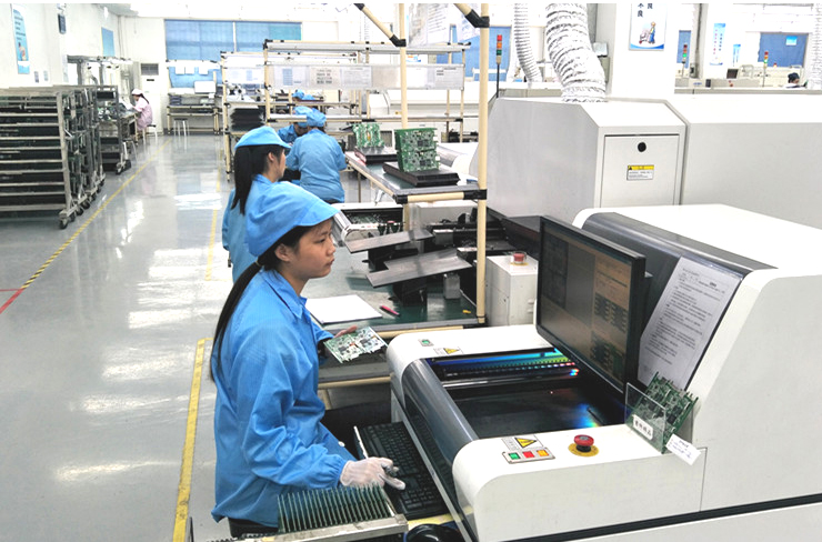
This guide walks through each stage of the SMT assembly process, explains what can go wrong at each, and shows where quality is actually controlled on a modern line.
The 5 Stages of SMT Assembly
Stage 1: Solder Paste Printing
A stainless steel stencil (typically 0.1–0.15 mm thick, laser-cut with electropolished apertures) is aligned over the bare PCB, and solder paste — a suspension of solder alloy particles (usually SAC305) in flux — is squeegeed through the stencil apertures onto each pad.
Key process controls: stencil alignment (±25 µm or better on modern lines), paste temperature (18–26°C), humidity (40–60% RH), and squeegee pressure. Industry data consistently attributes 50–70% of all SMT defects to the printing step — insufficient paste causes open joints, while excess paste causes bridging.
After printing, most lines run SPI (solder paste inspection), an optical check that measures paste volume, area, and height per pad. Catching a bad print before placement costs cents; catching it after reflow costs the whole board.
Stage 2: Component Placement
Pick-and-place machines pick components from reels, trays, or tubes using vacuum nozzles and place them onto the pasted pads at speeds of 15,000–100,000+ components per hour. Modern placement heads achieve ±25 µm accuracy, which is what makes 01005 passives and 0.35 mm-pitch BGAs manufacturable at all.
Three things matter here: the program (X/Y coordinates, rotation, and placement height per component), the feeder setup (wrong reel in wrong slot is among the most common factory errors), and nozzle condition. First-article inspection after setup confirms everything before volume placement begins.
Stage 3: Reflow Soldering
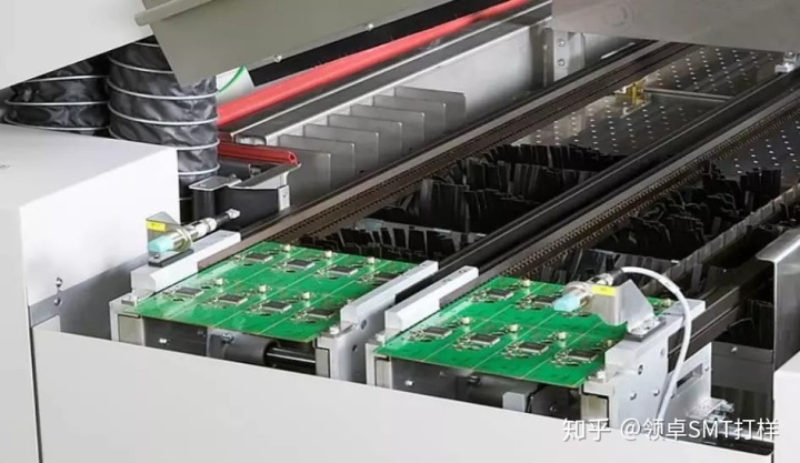
The populated board travels through a reflow oven with 6–10 individually heated zones, following a carefully measured temperature profile:
- Preheat (150–180°C, 60–120 s): evaporates solvents and activates the flux gradually, preventing thermal shock.
- Soak (60–120 s): equalizes temperature across all components, critical for large BGAs next to tiny passives.
- Reflow (peak 235–250°C for SAC305, time above liquidus 30–90 s): the solder melts, wets the pads and terminations, and forms the metallurgical joint.
- Cooling (controlled, ≤4°C/s): solidifies the joint; too-fast cooling creates grain stress and cracking.
A wrong profile is the second biggest source of defects: too little heat gives dull, unreliable joints; too much heat damages packages, delaminates boards, and "tombstones" small passives.
Stage 4: Inspection
Three inspection methods cover different defect classes:
- AOI (automated optical inspection): high-speed camera check for missing, misaligned, or polarity-reversed components, bridging, and insufficient joints. Catches ~90% of visible defects.
- X-ray inspection (AXI): sees inside BGA, QFN, and LGA packages where the joints are hidden, revealing voids, opens, and bridging under the package. Essential for any design with bottom-terminated components.
- Manual/visual IPC-A-610 sampling: human judgment on cosmetics and borderline calls, per the IPC acceptability standard.
Stage 5: Testing
Inspection confirms the board was built right; testing confirms it works. Common test stages: in-circuit test (ICT) for shorts/opens and component values, functional test (FCT) for real-world behavior, and programming/flashing where firmware is loaded as a final step. Our SMT assembly service includes AOI on every production lot, with ICT and functional test available as options.
What a Modern SMT Line Looks Like
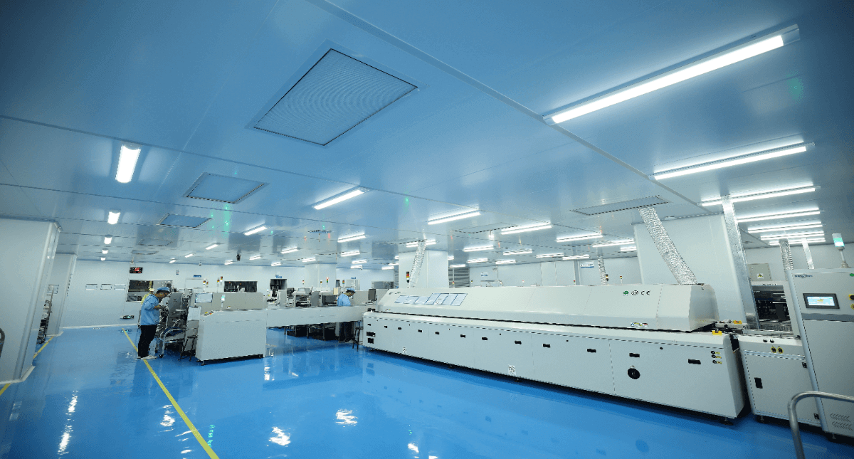
A production SMT line is a sequence of linked machines, each with one job, running at the speed of its slowest stage:
- Loader: stacks bare boards (or panels) and feeds them one by one onto the conveyor.
- Solder paste printer: the stencil printer described above, usually with automatic paste dispensing and wipe cycles to keep apertures clean.
- SPI machine: 2D or 3D solder paste inspection between printing and placement — the checkpoint that catches the majority of print defects before value is added.
- Pick-and-place machines: often two or more in sequence — a high-speed "chip shooter" for small passives (0201, 0402) at 30,000+ cph, then a precision multifunction machine for ICs, connectors, and odd-shaped parts.
- Reflow oven: 8–10 zone forced-convection oven with nitrogen option for oxidationsensitive parts.
- Unloader, then AOI: boards are collected and transferred to inspection, which may be inline (conveyor-fed) or offline batch.
Inline SPI plus AOI creates a closed feedback loop: when SPI trends show paste volume drifting on a specific pad, the line is stopped and the stencil is cleaned before hundreds of boards are affected. That feedback loop — not any single machine — is what separates a modern line from an old one.
For mixed-technology boards, a THT stage follows: either a wave solder machine for through-hole parts on the solder side, or selective soldering for boards that cannot tolerate wave exposure on the top side.
Where SMT Defects Actually Come From
| Defect | Typical root cause | Caught by |
|---|---|---|
| Solder bridging (shorts) | Excess paste, stencil aperture too large | AOI / ICT |
| Open joints | Insufficient paste, poor wetting, lifted pads | AOI / X-ray / ICT |
| Tombstoning | Asymmetric pad heating or paste deposit | AOI |
| Voiding under BGAs | Flux outgassing, bad profile | X-ray |
| Wrong component | Feeder setup error | First-article inspection / AOI |
| Head-in-pillow (BGA) | Paste/component oxidation, profile ramp too fast | X-ray |
Reading a Reflow Profile Report
Every production run should ride on a measured profile, not a default oven recipe. When your factory shares the profile report, check four numbers:
- Ramp rate: the slope from ambient to 150°C — 1–3°C/s is safe; faster ramps stress components and pop small packages.
- Time above liquidus (TAL): for SAC305, 30–90 s between 217°C and peak. Under-cured joints look dull and fail early; over-cured flux leaves residues and damages housings.
- Peak temperature: 235–250°C on the joint — and verify the profile was measured with a profiler board running through the actual conveyor, not taped to the belt.
- Delta across the board: the spread between the hottest and coldest joint on the same assembly. A delta over 15°C means the oven recipe is fighting your board design (heavy copper areas heat slowly) and warrants fixture or panel changes.
A factory that volunteers the profile report without being asked is one that runs controlled processes; treat it as a positive signal in supplier evaluation.
SMT vs Through-Hole: When Each Makes Sense
Pure SMT dominates modern assembly because it is fast, automatable, and enables double-sided dense boards. Through-hole (THT) survives where mechanical strength matters — connectors, transformers, large capacitors, anything that sees physical stress — and in high-power designs where the joint itself carries heat. Mixed-technology boards run both: SMT first, then THT by wave solder or selective soldering. A good assembly partner will flag during quote review if your design mixes the two, since it changes line setup and cost.
How to Prepare Your Design for Smooth SMT Assembly
- Provide a complete pick-and-place (Centroid) file with X/Y coordinates, rotation, and reference designators — it programs the placement machine directly.
- Keep fiducials: two (preferably three) 1 mm solid fiducials on the paste side, and panel fiducials if boards are panelized.
- Standardize component orientations in your library — inconsistent rotation conventions are a classic source of misplacement.
- Avoid placing tall components next to fine-pitch parts where the nozzle clearance fails.
- For BGAs, include via-in-pad or dogbone fanouts per your fabricator's rules, and specify X-ray inspection in your order.
FAQ
How long does SMT assembly take?
Pure assembly labor is fast — a few thousand boards can be placed and reflowed in hours. The real lead time is component sourcing and test setup: plan 2–5 working days for a typical production lot, or 48–72 hours for expedited prototype runs.
What is the difference between AOI and X-ray inspection?
AOI uses cameras to check visible joints and component placement; X-ray sees through packages to inspect hidden joints like BGA balls. AOI is standard on every lot; X-ray is used for bottom-terminated components or high-reliability orders.
Why do so many defects come from solder paste printing?
Because every subsequent step depends on the paste deposit being right: volume, position, and height. Small stencil misalignments or aperture blockages propagate into opens, shorts, and weak joints that only appear later in testing.
Can SMT handle both sides of the board?
Yes — standard flow is print/place/reflow the bottom side first, then flip the panel and repeat for the top side with heavier components restricted to the top. Fine-pitch and BGA parts almost always go on the second (top) pass.
Comment on this article here
-
No comment

Ripple
Hi everyone, I'm Ripple, Sales Director of KFPCBA Tech Ltd. If you are looking for a one-stop PCB and PCB assembly manufacturer in China, KFPCBA is your best choice! Please feel free to contact our team! Thanks!
Contact me now
Relevant content you may be interested in
Related articles